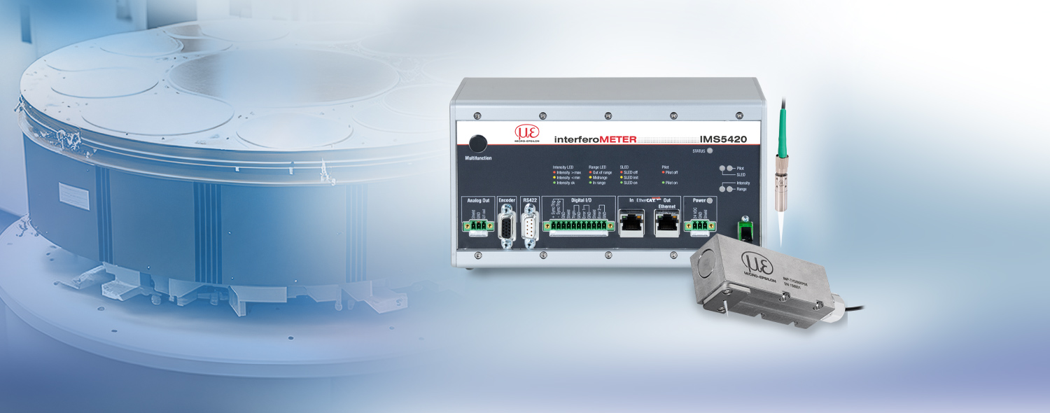
White light interferometer for high precision wafer measurement
The IMS5420 is a high-performance white light interferometer for non-contact thickness measurement of monocrystalline silicon wafers. The controller has a broadband superluminescent diode (SLED) with a wavelength range of 1,100 nm. This enables the thickness measurement of undoped, doped and highly doped SI wafers with only one measuring system and signal stability of less than 1 nm. Depending on the field of application, sensors with large offset distance and with air purge system are available.
Characteristics
- Nanometer-accurate thickness measurement of undoped, doped and highly doped wafers
- Multi-peak: acquisition of up to 5 layers with an SI thickness of 0.05 up to 1.05 mm
- High resolution in z-axis of 1 nm
- Measuring rate up to 6 kHz for fast measurements
- Ethernet / EtherCAT / RS422 / PROFINET / EtherNet/IP
- Easy parameterization via web interface
Precise wafer thickness measurement
Due to the optical transparency of silicon wafers in the wavelength range of 1,100 nm, the IMS5420 interferometers can precisely detect the thickness. In this wavelength range, both undoped silicon and doped wafers provide sufficient transparency. Therefore, wafer thicknesses up to 1.05 mm can be detected. The measurable thickness of the air gap is even up to 4 mm.
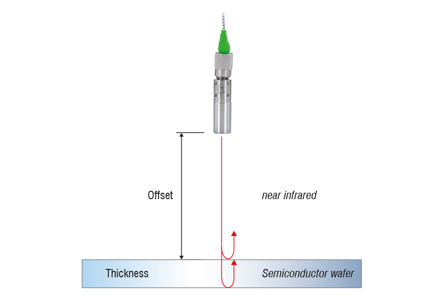
The IMS5420 interferometer enables the thickness measurement of undoped, doped and highly doped silicon wafers and thus offers a wide range of applications. This wafer thickness measuring system is ideal for the measurement of monocrystalline silicon wafers with a geometric thickness of 500 to 1050 µm and a doping of up to 6 m Ω cm. Despite decreasing transparency with increasing doping, thicknesses up to 0.8 mm can still be measured even of highly doped wafers.
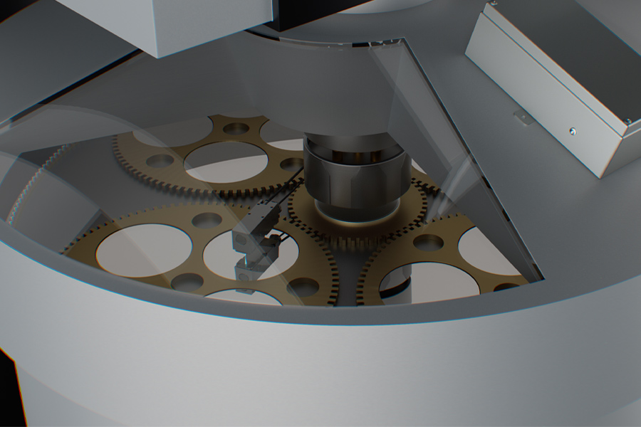
Precise thickness measurement during lapping
In wafer fabrication, a crystalline silicon ingot is sawn into thin slices of about 1 mm. The wafers are then ground and lapped to obtain the desired thickness and surface finish. For stable, reproducible process control, interferoMETER systems for inline thickness measurement are integrated directly into lapping and grinding machines. The detected thickness values are used for machine control as well as for quality control of each single wafer.
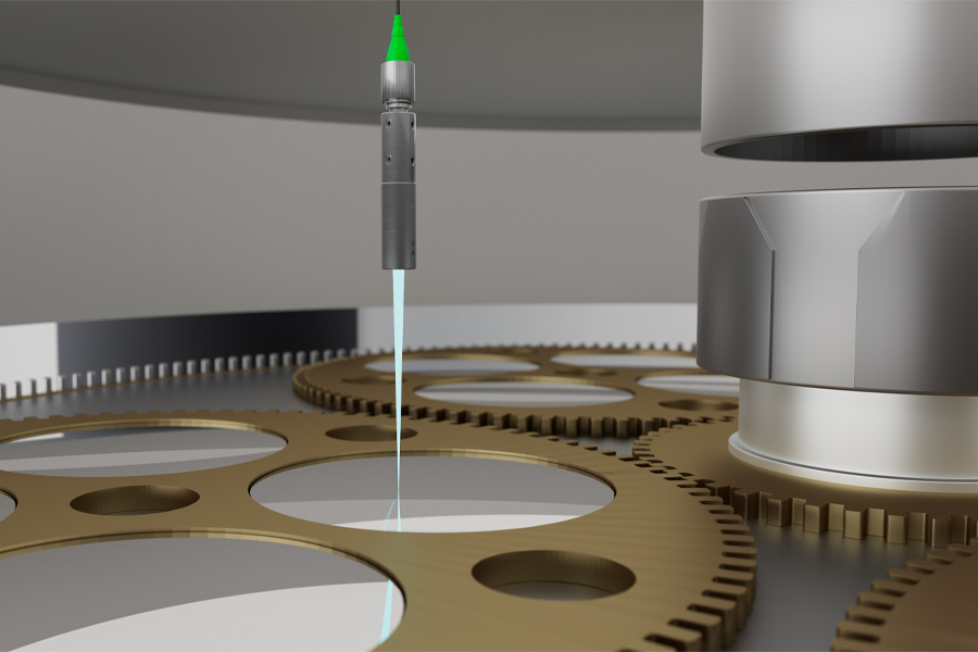
Compact IMP-NIR-TH24 sensor
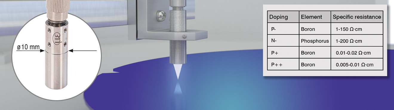
With its slim diameter of just 10 mm and its large working distance of 24 mm, the IMP NIR TH24 is ideal for retrofitting in existing systems. The adjustable mounting adapter (JMA) significantly simplifies the integration, as even minor mounting deviations or inclined positions can be reliably compensated for. Both the sensor and the fiber optic cable are available in UHV design on request.
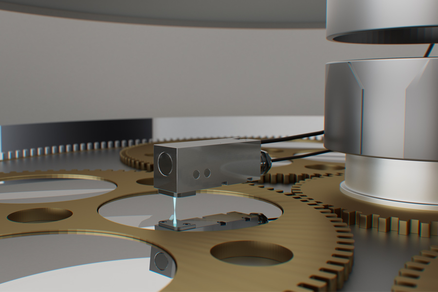
NEW: Robust IMP-NIR-TH3/90/IP68 sensor
The IMP-NIR-TH3/90/IP68 expands the sensor portfolio with a high-performance sensor for particularly demanding installation situations and harsh environmental conditions. This sensor impresses with a 90° beam path and a small working distance of just 3 mm – ideal for very tight installation situations. Due to its robust housing (IP68), the sensor is also suitable for particularly demanding applications, such as slurry grinding. The integrated air purge device keeps the beam path continuously free of contamination and thus enables permanent measurement accuracy – even in heavily contaminated environments.
Numerous models for demanding measurement tasks
| Model | Working distance / measuring range | Linearity | Number of measurable layers | Fields of application |
|---|---|---|---|---|
| IMS5420-TH | Working distance IMP-NIR-TH24 approx. 24 mm (21 ... 27 mm) | IMP-NIR-TH3/90/IP68 approx. 3 mm (1 ... 6 mm) / 0.05 ... 1.05 mm (for silicon / n=3.82), 0.2 ... 4 mm (for air, n=1) |
< ±100 nm | 1 layer | Inline thickness measurement, e.g. after grinding or polishing. |
| IMS5420MP | < ±100 nm for one layer < ±200 nm for additional layers |
up to 5 layers | Inline thickness measurement, e.g. for quality control of the layer thickness after coating. | |
| IMS5420/IP67 | Working distance IMP-NIR-TH24 approx. 24 mm (21 ... 27mm) / 0.05 ... 1.05 mm (for silicon / n=3.82), 0.2 ... 4 mm (for air, n=1) |
< ±100 nm | 1 layer | Industrial inline thickness measurement during lapping and grinding. |
| IMS5420/IP67MP-TH | < ±100 nm for one layer < ±200 nm for additional layers |
up to 5 layers | Industrial inline thickness and multilayer measurement during lapping and grinding. |
Modern interfaces for integration into machines and systems
The controller offers integrated interfaces such as Ethernet, EtherCAT and RS422 as well as additional encoder connections, analog outputs, synchronization inputs and digital I/Os. When you use Micro-Epsilon's interface modules, PROFINET and EthernetIP are available. This allows the interferometer to be integrated into all control systems and production programs.